Plastic Ball Grid Array, PBGA

PBGA Package Dimensions
PBGA [Plastic Ball Grid Array] is a surface mount package, made of plastic, that uses solder balls to attach to the Printed Wiring Board [PWB] or BGA socket. Note that the graphic also uses the acronym PGA which would refer to Plastic Grid Array. A PBGA would be a sub style of the more general BGA acronym, in that a BGA could also refer to a Plastic BGA.
BGA: is a Surface Mount Package, and there are a number of styles;
LBGA: Low-Profile Ball Grid Array
CBGA: Ceramic Ball Grid Array
As with any package style, there are a number of different variations, both in package material, physical size, and shape, but only a few are listed here.
There are also a number of different ball patterns and body shapes. The BGA package shown above is odd only because of the body shape, being rectangular instead of square, but still contains a full Ball Grid Array.

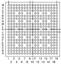
PBGA Ball Pattern Example
The square PBGA package shown above are more common, note the actual Ball Grid Array could change even if two ICs are the same physical size. In that there is no define pattern the solder balls need to adhere to. In fact to assist in routing, solder balls may be omitted by the manufacturer, from the package producing an odd grid array [as found in the PBGA package shown to the left].
Design Hint; Unused solder pads could be omitted from the layout to produce a bit more routing room between the solder balls. However the draw-back of not providing a solder pad for a unused ball would be that that solder ball could not be used at a later time [having no solder pad to attach a mag-wire to]. Note; some engineering departments refer to a wire used to repair or change a board design as a mag-wire or white-wire, with other terms possible.