2N6249T3 Temperature-Power Derating Curve
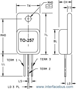
NPN Power Transistor. Package, TO-257AA [TO-254AA, TO-3 metal Can].

2N6249T3 Transistor Temperature-Power Derating Curve
The chart details the maximum allowable power dissipation with increasing component case temperature. Maximum operational power dissipation is achievable at 25C. However above 25C the maximum package dissipation, or power, must be reduce to insure that the devices junction temperature remains constant. The higher the case temperature is increased the lower the allowable power dissipation, as depicted in the curves. Decreasing a devices operational limits as temperature is increased is called derating, in this case derating a devices operational power dissipation vs increasing case temperature. The graph above depicts the derating of a 2N6249 transistor in a TO-257 package [2N6269T3].
The blue curve shows the maximum junction temperature, after which damage to the semiconductor might occur. The black line only serves to show the operating curve at which the electrical characteristics were recorded. The green lines show the power and temperature range that a proper design should operate at or within.
2N6249 Transistor Derating Curves
Additional Transistor Derating Curves for other devices.
Temperature derating is a standard design practice for electrical engineers.
Refer to MIL-PRF-19500/510; Silicon Semiconductor Device, NPN Power Transistor. Transistor Types; 2N6249, 2N6249T1, 2N6249T3, 2N6250, 2N6250T1, 2N6250T3, 2N6251, 2N6251T1, 2N6251T3,
JAN, JANTX, JANTXV, JANS, JANHC, and JANKC.
Semiconductor Packages; TO-3, TO-254AA & TO-257AA.
The mil spec covers all three packages listed, but the power derating curve shown above only covers the TO-257AA package. The revision level for the specification is not listed, as they may change at any time.
Maximum Ratings 250C [Operational]:
Collector Emitter Voltage = 200 volts dc
Collector Base Voltage = 300 volts dc
Emitter Base Voltage = 6.0 volts dc
Collector Current = 10 amp dc
Base Current = 5 amps dc
Power Dissipation = 4 Watts [Ta = 250C]
Power Dissipation = 125 Watts [Tc = 250C]
Operating Temperature = -65 to +2000C
Storage Temperature = -65 to +2000C
TO-257 Terminals: Lead 1, Base. Lead 2, Collector. Lead 3, Emitter
The terminals are isolated from the metal tab.