General Engineering Terms
"A"
"B"
"C",
"D",
"E",
"F",
"G",
"H",
"I",
"J",
"K",
"L",
"M",
"N",
"O",
"P"
"Q",
"R",
"S",
"T",
"U",
"V",
"W",
"X",
"Y",
"Z"
Op Amp Circuits
There a few general circuit configuration that are used over and over in many types of more complicated circuits, as well as the most simplistic Op-Amp circuits. The page covers the most basic configurations for operational amplifier. Unless stated otherwise the amplifiers are assumed to be general purpose 741 Op-Amps, or similar devices. Device pin outs are not shown, so the operational amplifier could be a single device or one of two or more from a dual or quad package.
When circuit diagrams are used to represent basic Op-Amp functions in many cases the input resistor is labeled Ri and the feedback resistor is labeled Rf. Much of this site uses R1 to represent Ri and R2 to indicate Rf, which fits better when adding more resistors, resulting in the next one being labeled as R3, R4 and so on.
Inverting Op-Amp
The inverting amplifier is one of the most basic circuit configurations. Having an input resistor R1 [or Ri] and a feedback resistor R2 [or Rf]. The output voltage is just the inversion of the input multiplied by the ratio of the two resistors. The equation is |
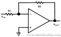 Inverting Amplifier |
Non-Inverting Op-Amp
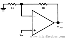 Non-Inverting Amplifier | The non-inverting amplifier is the second most basic circuit configuration. Having an input resistor R1 and a feedback resistor R2. The output voltage is again the input multiplied by the ratio of the two resistors. The equation is |
Summing Op-Amp
The summing amplifier combines or adds additional inputs to the inverting amplifier. In this case the 3 inputs are summed together [the number of inputs is not fixed]. The output than becomes the inverted input multiplied by the feedback resistor [R4 in this case], and each of the input resistors. R5 is a compensation resistor to off-set the bias current difference. The output equation is |
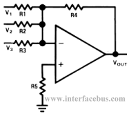 Summing Amplifier |
Difference Op-Amp
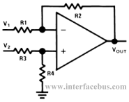 Difference Amplifier | The difference amplifier combines the functions of the inverting amplifier with the non-inverting amplifier. The output equation is |
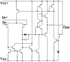
Op-Amp Package Options
The common package options for a single or dual operation amplifier is an 8-pin package. Dual or quad Op Amps are found in a 16-pin package. The through-hole packages may be either Plastic DIP Package, or Ceramic DIP Package [for military and space applications], while the surface mount versions will be in a SOIC Package. Older versions may be found using a round metal can 8-Lead TO-5 Case.
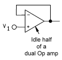
Unused Inputs
Packages with more than one amplifier may need to have one of the amplifier tied off if not being used. Any unused Op-amp should be configured per the diagram to the right, tying the output to the negative input pin. For example the LM3900 OpAmp is a quad package, unused devices should be connected as shown in the graphic.
Off-Set Null
Depending on the Op Amp used, off-set adjust pins may be offered to compensate for any error caused by input currents shifting the output. Refer here for different methods for OpAmp Off-Set Null Adjustment.
Frequency Compensation
The LM101 is an example of an Op Amp which has two pins for Frequency Compensation. The pins allow the connection of an external frequency compensating network, normally just a capacitor, to tailor the characteristics to the particular application. While other Op-amps [an LM107 for example] have to rely on their fixed internally compensated amplifiers, having no adjustment.
An operational amplifier should also have a bypass capacitor from each power supply pin to ground.