Definitions of Engineering Terms
"A",
"B",
"C",
"D",
"E",
"F",
"G",
"H",
"I",
"J",
"K",
"L",
"M",
"N",
"O",
"P",
"Q",
"R",
"S",
"T",
"U",
"V",
"W",
"X",
"Y",
"Z"
Differential Transistor Amplifier
A differential amplifier is an amplifier that has two inputs and produces an output that is a function of the difference between the two inputs. A differential amplifier should produce a zero output when both inputs are identical.
The following is in the same progression as the first page covering the Single Input Differential Amplifier, however this topic covers the dual input version or a true differential amplifier. The same circuit is used to describe the operation, although the configuration is changed slightly.
No transistor part is selected, but a 2N3055 NPN Transistor could be used for medium to high power applications. The link provides electrical characteristics, guidelines for high temperature operation and package data. As with the previous example, any transistor would be suitable as long as its matches the voltage and current range determined by the voltage supply and resistor values.
Emitter Follower
The Emitter follower is shown only because of the operation between the input base signal and the resultant output taken from the emitter. The configuration produces an output that follows the input signal but reduced by the diode drop across the transistor. As the input signal becomes positive the transistor conducts and generates a signal across the emitter resistor. | 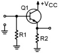 Emitter Follower |
The output signal follows the input as long as the input voltage is above the diode drop of the Base-Emitter junction. The emitter follower is used as a starting point because it produces an output in phase with the input and helps with the basic understanding of the differential amplifier discussed below.
Single Input Differential Amplifier
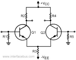 Single Input | In regards to this description each transistor is configured as a common emitter amplifier, with resistor R3 being the emitter resistor [of both transistors]. So an input to Q1 develops a signal across R3. An input to Q2 also generates a signal across R3. |
Then a signal applied to Q1 changes the voltage at R3, which is a change in the voltage at the emitter of Q2 effecting that transistors current. And the reverse is true, as an input to Q2 changes the voltage across R3, which has an effect on the current through Q1.
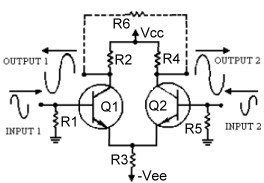 Combined output Amplifier | As with the previous example, the outputs maybe combined to a single load. In this case the load resistor R6 combines both outputs producing an output that is twice either output and in phase with input number 1. |
What wasn't mentioned on the first page is that the load resistor isn't grounded, its floating. It's the same circuit as above, with each individual output being 180 degrees out of phase with one another. As with the single input single output circuit; the output at Q2 is in phase and an amplified version of the signal on the base of Q1. In addition, now the output of Q1 is an amplified version of the signal at the base of Q2, also in phase. Or looking at it another way, the transistor output is a 180 degree phase shifted, amplified signal of the input to the transistor.
The two signals are combined by adding the two 180 degree phase shifted signals across R6. The output developed across the load resistor is equal to twice either signal. Of course the actual amplitude of the signals generated by either transistor depends on the gain of the transistor.
Related Transistor Data
Transistor Specifications & Characteristics
Electrical specifications and thermal data.
Transistor Manufacturers & Vendors
List of companies making transistors and the types the makes
Transistor Package Styles
Different types of transistor packages and descriptions
Transistor Definitions & Jargon
Terms and acronyms used with transistors
Basic Transistor Configurations
Brief descriptions of the general transistor setups.