The approximate board size. 5.375" x 1.375"
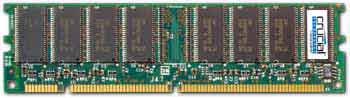
Personal Computer Memory Module description, 168-pin Registered SDRAM
DIMM Pin out.
The 168-pin DIMM have 84 pins per PWB side.
The Front Side board pinout contains left side pins 1-42, and right side pins 43-84.
The Back Side board pinout has left side pins 85-126, and right side pins 127-168.
Buffered 168-pin DIMM memory modules would be found in servers.
Front-Side 168-pin Buffered Pin Out
| Pin # | Pin name | Pin Description |
|---|---|---|
| 85 | VSS | Ground |
| 86 | DQ32 | Data 32 |
| 87 | DQ33 | Data 33 |
| 88 | DQ34 | Data 34 |
| 89 | DQ35 | Data 35 |
| 90 | VCC | +5 VDC or +3.3 VDC |
| 91 | DQ36 | Data 36 |
| 92 | DQ37 | Data 37 |
| 93 | DQ38 | Data 38 |
| 94 | DQ39 | Data 39 |
| 95 | DQ40 | Data 40 |
| 96 | VSS | Ground |
| 97 | DQ41 | Data 41 |
| 98 | DQ42 | Data 42 |
| 99 | DQ43 | Data 43 |
| 100 | DQ44 | Data 44 |
| 101 | DQ45 | Data 45 |
| 102 | VCC | +5 VDC or +3.3 VDC |
| 103 | DQ46 | Data 46 |
| 104 | DQ47 | Data 47 |
| 105 | CB4 | Parity/Check Bit Input/Output 4 |
| 106 | CB5 | Parity/Check Bit Input/Output 5 |
| 107 | VSS | Ground |
| 108 | NC | No Connection |
| 109 | NC | No Connection |
| 110 | VCC | +5 VDC or +3.3 VDC |
| 111 | /CAS | - |
| 112 | /CAS4 | Column Address Strobe 4 |
| 113 | /CAS5 | Column Address Strobe 5 |
| 114 | /S1 | - |
| 115 | /RAS | - |
| 116 | VSS | Ground |
| 117 | A1 | Address 1 |
| 118 | A3 | Address 3 |
| 119 | A5 | Address 5 |
| 120 | A7 | Address 7 |
| 121 | A9 | Address 9 |
| 122 | BA0 | - |
| 123 | A11 | Address 11 |
| 124 | VCC | +5 VDC or +3.3 VDC |
| 125 | Ck1 | - |
| 126 | A12 | Address 12 |
| Pin # | Pin name | Pin Description |
|---|---|---|
| 127 | VSS | Ground |
| 128 | CKE0 | - |
| 129 | /S3 | Column Address Strobe 3 |
| 130 | /CAS6 | Column Address Strobe 6 |
| 131 | /CAS7 | Column Address Strobe 7 |
| 132 | A13 | Address 13 |
| 133 | VCC | +5 VDC or +3.3 VDC |
| 134 | NC | No Connection |
| 135 | NC | No Connection |
| 136 | CB6 | Parity/Check Bit Input/Output 6 |
| 137 | CB7 | Parity/Check Bit Input/Output 7 |
| 138 | VSS | Ground |
| 139 | DQ48 | Data 48 |
| 140 | DQ49 | Data 49 |
| 141 | DQ50 | Data 50 |
| 142 | DQ51 | Data 51 |
| 143 | VCC | +5 VDC or +3.3 VDC |
| 144 | DQ52 | Data 52 |
| 145 | NC | No Connection |
| 146 | NC | No Connection |
| 147 | NC | No Connection |
| 148 | VSS | Ground |
| 149 | DQ53 | Data 53 |
| 150 | DQ54 | Data 54 |
| 151 | DQ55 | Data 55 |
| 152 | VSS | Ground |
| 153 | DQ56 | Data 56 |
| 154 | DQ57 | Data 57 |
| 155 | DQ58 | Data 58 |
| 156 | DQ59 | Data 59 |
| 157 | VCC | +5 VDC or +3.3 VDC |
| 158 | DQ60 | Data 60 |
| 159 | DQ61 | Data 61 |
| 160 | DQ62 | Data 62 |
| 161 | DQ63 | Data 63 |
| 162 | VSS | Ground |
| 163 | CK3 | |
| 164 | NC | No Connection |
| 165 | SA0 | Serial Address 0 |
| 166 | SA1 | Serial Address 1 |
| 167 | SA2 | Serial Address 2 |
| 168 | VCC | +5 VDC or +3.3 VDC |
Data width is 64 bits per memory stick [the front side 84 pins are not connected together with the back side 84 pins]
SIMM: Single Inline Memory Module
DRAM: Dynamic Random Access Memory
SO DIMM: Small Outline Dual Inline Memory Module
SDRAM:: Synchronous DRAM (Random Access Memory), Synchronous to
Positive Clock Edge.
FPM:Fast Page Mode: (asynchronous) Obsolete, faster than normal
DRAM, used in 386/486 computers.
EDO: Extended Data Out: (asynchronous) A superset of FPM, just
faster than FPM.
All 168 pin DIMMs use either 66MHz SDRAM, PC100 SDRAM, PC133 SDRAM, EDO
or FPM memory.
168 pin DIMMs have two alignment notches as shown.
The left most notch [key-way] determines the DRAM type.
If the notch is
centered then the memory module is Buffered DRAM [EDO or Fast Page].
If the notch is off-set to the right then the memory module is either a
un-buffered DRAM/SDRAM DIMM or a buffered SDRAM DIMM.
The center notch
determines the voltage. If the notch is centered then the DIMM operates
off 3.3 volts.
Back to the main Computer Memory
Modules information page. For electronic device manufacturers see one
of these pages:
Memory IC manufacturers [individual memory ICs]
Memory Module manufacturers [memory sticks]
Memory Module Acronyms [phrases used with memory sticks]
IC Memory Acronyms [phrases used with IC memory]
Additional electronic Equipment manufacturers may be found by selecting the OEM Equipment icon below.
Component manufacturers, including memory ICs, may be found by selecting the Components icon below.
Editor note; I'm not going to say that 168 pin DRAM buffered DIMMs are obsolete, but they are out-dated.
Of course the pin outs remain valid regardless of the age of the Memory Module.
In fact, at this point the pinouts, pin descriptions and signal names are set in stone.
Regardless of the continued usage of 168-pin DRAMs, they were Obsoleted by Double Data Rate memory.
More over, the current Memory Module format is DDR3, or the third generation of DDR, making this memory style very old.
So 168 pin DRAM buffered DIMM sticks should not be used in new designs.
Navigation: Engineering Home > OEM Equipment Vendors > Computer Gear > Memory Modules > Memory Module Pinout > 168 pin DIMM memory stick.
 | |||||||
| Home | |||||||
 |
 |
 |
 |
 |
 |
 |
 |
| Distributors | Components | Equipment | Software | Standards | Buses | Design | Reference |