Technical Engineering Definitions
"A"
"B"
"C",
"D",
"E",
"F",
"G",
"H",
"I",
"J",
"K",
"L",
"M",
"N",
"O",
"P"
"Q",
"R",
"S",
"T",
"U",
"V",
"W",
"X",
"Y",
"Z"
Transistor Envelope Detector
The basic diode peak detector was covered on a previous topic, entitled Peak Detector. The diode envelope detector is shown again for convenience. The same waveforms used in the previous example are also shown to the right. This page covers transistors used as envelope detectors. |
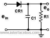 Peak Detector |
Two different circuits are provided as examples. Both circuits have an identical function and are used as envelope detectors for an Amplitude Modulated [AM] signal. The primary difference is how the transistor is used as an amplifier, a Common Base in one circuit and a Common Emitter in the other. The components required by the amplifier change in order to support the configuration of the transistor. The different ways to use or configure a transistor is shown, with different examples, on the Transistor Terms page.
A general definition of the implementation may be found under the heading or term AM Receiver which contains an overview.
Common Base Envelope Detector
The term amplifying detector is used in this case, because the circuit is both an envelope detector and an amplifier. Of course the diode detector used in the previous example would not be considered an amplifier.
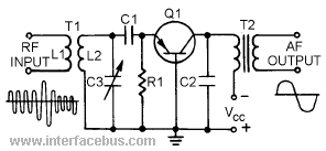
Common-Base Envelope Detector
The amplitude modulated RF input is applied to the primary [L1] of transformer T1.
The Emitter-Base junction forms an equivalent diode detector as covered before. The Collector side of the transistor serves as the amplifier section, so the circuit is the same as a diode detector followed by an amplifier. The input section comprised of T1 and capacitor C3 form a tuning circuit which is adjusted to the frequency of the incoming modulation envelope. [or its center frequency]. The adjustable capacitor is used to tune the LC circuit [C3 & L2] to the desired frequency.
Resistors R1 and C1 only serve to bias the transistor and set the DC bias point of the Emitter circuit. R1 provides the DC bias; however the combination of R1 and C1 act as a filter producing a varying DC voltage to the input of the transistor. The voltage resulting from the filter follows the rises and falls of the incoming envelope. The varying dc bias on the Emitter junction causes an identical, but amplified, voltage on the Collector of the transistor.
The detected envelope which happens to be the desired Audio Frequency [AF] is passed to the output. The Collector voltage is applied to the transistor through the output transformer [T2]. The primary of T2 forms the load of the transistor. Capacitor C2 is an RF bypass capacitor. The load of the circuit segment is the transformer, but the ultimate output is connected to the secondary of T2 and not shown.
Common Emitter Envelope Detector
An alternative circuit to detecting the envelope of an AM signal is shown below. This circuit approach uses a Common-Emitter transistor configuration. The term common-emitter detector might be used to describe the circuit. Common Emitter refers to the fact the Emitter leg of the transistor is common to both the input circuit [Base-Emitter] and the output circuit [Collector-Emitter].
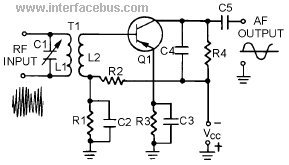
Common-Emitter Envelope Detector
As before the amplitude modulated input is applied to transformer T1. However this time the tuned circuit [C1 & L1] is found on the primary of the transformer. The adjustable capacitor is tuned to the desire frequency of the modulated wave [audio frequency]. The transformers secondary couples the signal to the Base of the transistor. Resistors R1 and R2 form a voltage divider which supply a DC bias to the Base of the transistor. Capacitor C2 [and C3] is a bypass capacitor which shorts out resistor R1 for RF signals.
The Emitter-Base junction of the transistor acts as the detection diode. The incoming voltage is developed across R1, of the R1/R2 voltage network. The varying [AF] frequency voltage is applied to the Base of the transistor and amplified by the Collector circuit.
The output signal is developed across resistor R4, which again is bypassed for RF by capacitor C4. Capacitor C5 is simply a DC blocking capacitor which blocks the DC voltages [Vcc] needed by transistor Q1 to function from reaching the next circuit down the line.


