Technical Engineering Definitions
"A"
"B"
"C",
"D",
"E",
"F",
"G",
"H",
"I",
"J",
"K",
"L",
"M",
"N",
"O",
"P"
"Q",
"R",
"S",
"T",
"U",
"V",
"W",
"X",
"Y",
"Z"
Transistor AM Modulator
There are a number of topics covered that are related to AM modulation, starting with a basic block diagram of an AM Receiver, which shows the relationship of the different subsystems. What isn't covered, is at least touched-on using the links to the engineering dictionary above. In regards to an AM receiver another topic deals with the basic Diode Detector, and another gives an example and description of an Envelope Detector.
This page offers another example of a transistor modulator designed to modulate signals onto an RF carrier. This particular circuit injects both the audio signal and RF signal into the Base circuit. A Base-Injection Modulator. An alternative approach to the one discussed below is the Collector Injection Modulator Circuit which is almost an identical approach but with a slightly different circuit configuration.
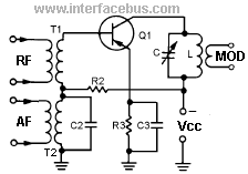
Base Injection Modulator Circuit
An Amplitude Modulator [AM] circuit, shown below, receives an RF carrier [RF Input] and modulates that signal with the Audio Frequency [AF] signal to produce a modulated signal, which is the circuits output.
The circuit is called a base injection modulator because the modulating signal is injected into the Base side of the transistor circuit, along with the carrier wave. The PNP transistor [Q1] is configured as a common-emitter circuit. The transistor circuit receives its input via the Base-Emitter side of the device and outputs the signal on the collector-emitter side, with the Emitter terminal being common to both input and output circuits. The voltage supply [Vcc] used to power the transistor is setup to supply a negative voltage to the circuit. Of course an NPN transistor would work just as well, as long as the voltage polarity is reversed.

Base-Injection AM Circuit
The Radio Frequency [RF] signal is applied to the primary side of T1, and coupled through the secondary to the Base of the transistor. The Base is biased by the resistor voltage divider formed by R1 and R2. The resistors fix the static voltage with no signal applied.
The modulating signal [AF input] is applied to the lower leg of the voltage divider, R1. As the voltage varies on the incoming modulating signal, it causes the voltage across R1 to vary. The modulating signal adds or subtracts to the static voltage developed by the resistors. This differs from the Collector Injection Modulator and allows for smaller signals to be used, because they will than be amplified by the transistor.
Capacitor C1 only acts as a DC blocking capacitor to prevent any DC bias voltage [originating from the AF portion of the circuit] from changing the set-point of the Base circuit. Capacitor C2 is an RF bypass capacitor that effectively shorts out R2, which is only needed to set the DC bias point.
The output side of the transistor is biased by resistor R3, which is also bypassed by an RF capacitor [C3]. The [series-fed] Tank Circuit comprised of the capacitor and inductor produce the output modulating signal. The variable capacitor is adjusted to the frequency of the RF carrier wave.
Base Injection Coupling Methods
The circuit above uses capacitive coupling to inject the audio frequency signal [AF Input] into the Base of the transistor. The transistor circuit to the right represents another alternative. That circuit uses transformer couplings to inject the AF signal. Other than the method of coupling, the two circuits are basically identical.